Spectroscopy
Spectroscopy is a branch of science concerned with the investigation and measurement of spectra produced when matter interacts with or emits electromagnetic radiation.
Spectroscopy the analysis of the interaction between matter and any portion of the electromagnetic spectrum. Traditionally, spectroscopy involved the visible spectrum of light, but x-ray, gamma, and UV spectroscopy also are valuable analytical techniques. Spectroscopy may involve any interaction between light and matter, including absorption, emission, scattering, etc.
Data obtained from spectroscopy is usually presented as spectrum (plural: spectra) that is a plot of the factor being measured as a function of either frequency or wavelength.
Emission spectra and Absorption spectra are common examples.
There are different spectroscopy techniques using:
-
Optical like UV-VIS, IR etc.
-
X-ray fluorescence and spectroscopy like XPS, UPS etc
-
Raman Spectroscopy and Imaging using Raman effect.
-
Nuclear Magnetic Resonance (NMR) etc.,
One of the important part of Spectroscopy is XPS or ESCA.
XPS/ESCA:
X-ray photoelectron spectroscopy (XPS) is also known as ESCA (Electron Spectroscopy for Chemical Analysis) emphasize the chemical (rather than merely elemental) information that the technique provides.
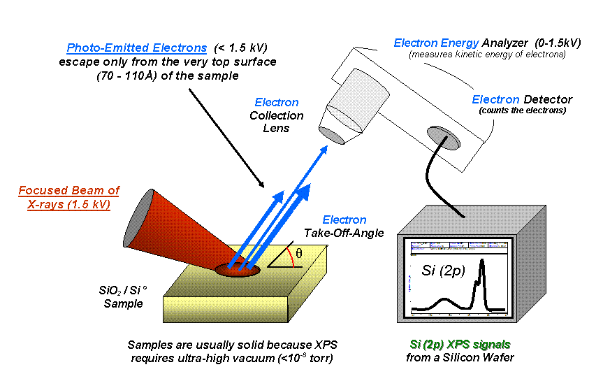
X-ray photoelectron spectroscopy (XPS) is a surface-sensitive quantitative spectroscopic technique that measures the elemental composition at the parts per thousand range, chemical state and electronic state of the elements that exist within a material. XPS spectra are obtained by irradiating a material with a beam of X-rays while simultaneously measuring the kinetic energy and number of electrons that escape from the top 0 to 10 nm of the material being analyzed. XPS requires high vacuum (P ~ 10−8 millibar) or Ultra-high vacuum (UHV; P < 10−9 millibar) conditions, although a current area of development is ambient-pressure XPS, in which samples are analyzed at pressures of a few tens of millibar.
XPS can be used to analyze the surface chemistry of a material in its as-received state, or after some treatment, for example: fracturing, cutting or scraping in air or UHV to expose the bulk chemistry, ion beam etching to clean off some or all of the surface contamination (with mild ion etching) or to intentionally expose deeper layers of the sample (with more extensive ion etching) in depth-profiling XPS, exposure to heat to study the changes due to heating, exposure to reactive gases or solutions, exposure to ion beam implant exposure to ultraviolet light.
-
In principle XPS detects all elements. In practice, using typical laboratory-scale X-ray sources, XPS detects all elements with an atomic number (Z) of 3 (lithium) and above.
-
Detection limits for most of the elements (on a modern instrument) are in the parts per thousand range all though detection limits of parts per million (ppm) are possible, but require special conditions: concentration at top surface or very long collection time (overnight).
-
XPS is routinely used to analyse inorganic compounds, metal alloys, semiconductors, polymers, elements, catalysts, glasses, ceramics, paints, papers, inks, woods, plant parts, teeth, bones, medical implants, bio-materials, viscous oils, glues, ion-modified materials and many others.
https://en.wikipedia.org/wiki/X-ray_photoelectron_spectroscopy
Ultra-violet photoemission spectroscopy (UPS)
Ultraviolet photoelectron spectroscopy (UPS) refers to the measurement of kinetic energy spectra of photoelectrons emitted by molecules which have absorbed ultraviolet photons, in order to determine molecular orbital energies in the valence region.
Auger Electron Spectroscopy(AES)
Auger electron spectroscopy (AES) is a commonly used analytical technique specifically in the study of surfaces and, more generally, in the area of material science. Underlying the spectroscopic technique is the Auger effect, which is based on the analysis of energetic electrons emitted from an excited atom after a series of internal relaxation events. Until the early 1950s Auger transitions were considered nuisance effects by spectroscopists, not containing much relevant material information, but studied so as to explain anomalies in x-ray spectroscopy data. Since 1953 however, AES has become a practical and straightforward characterization technique for probing chemical and compositional surface environments and has found applications in metallurgy. Gas-phase chemistry and microelectronics industry.
Imaging/Microscopy
From time immemorial imagination and imaging followed each other. Imagination lead to technology and better tools of imaging. These better tools of imaging fuelled further imaginations. Imaginations lead to technology and innovations. Quite a few techniques have emerged over the years as tools of imaging and microscopy. Some of the techniques used for imaging are:
1. Optical/Light microscopy – various wavelengths in the visible spectrum range.
2. X-ray: from earliest x-ray medical imaging to today’s X-ray tomography
3. Electron Microscopy like SEM/TEM, LEEM/PEEM whole range.
3. Scanning Probe Microscopy (SPM): Whole range like STM, AFM, MFM, EFM list is simply endless.
4. Raman microscopy/spectroscopy.
Scanning Probe Microscopy (SPM)
Scanning probe microscopy (SPM) is a branch of microscopy that forms images of surfaces using a physical probe that scans the specimen. SPM was founded in 1981, with the invention of the Scanning Tunnelling microscope (STM), an instrument for imaging surfaces at the atomic level. The first successful scanning tunneling microscope experiment was done by Binnig and Rohrer. The key to their success was using a feedback loop to regulate gap distance between the sample and the probe.
Many scanning probe microscopes can image several interactions simultaneously. The manner of using these interactions to obtain an image is generally called a mode.
The resolution varies somewhat from technique to technique, but some probe techniques reach a rather impressive atomic resolution. This is due largely because piezoelectric actuators can execute motions with a precision and accuracy at the atomic level or better on electronic command. This family of techniques can be called "piezoelectric techniques". The other common denominator is that the data are typically obtained as a two-dimensional grid of data points, visualized in fast color as a computer image.
https://en.wikipedia.org/wiki/Scanning_probe_microscopy
SPMs can be in ultra-high vacuum (UHV) or in ambient or in some atmosphere like liquid, gas or high temperature or low temperature.
Techniques and modes are exhaustive and new modes are being added frequently. Common to all these modes and techniques are physical probe (called tip) mechanically scanning or probing the surface.
Electron Microscopy
An electron microscope is a microscope that uses a beam of accelerated electrons as a source of illumination. As the wavelength of an electron can be up to 100,000 times shorter than that of visible light photons, electron microscopes have a higher resolving power than light microscope and can reveal the structure of smaller objects. A STEM (scanning transmission EM has achieved better than 50pm resolution in annular dark-field imaging mode and magnifications of up to about 10,000,000x whereas most light microscopes are limited by diffraction to about 200 nm resolution and useful magnifications below 2000x.
Electron microscopes have electron optical lens systems that are analogous to the glass lenses of an optical light microscope.
Family electron microscopes are exhaustive.
https://en.wikipedia.org/wiki/Electron_microscope
Low Electron Energy Microscope (LEEM)
Low-energy electron microscopy, or LEEM, is an analytical surface science technique invented by Ernst Bauer in 1962, however, not fully developed (by Ernst Bauer and Wolfgang Telieps) until 1985. LEEM is a technique used by surface scientists to image atomically clean surfaces, atom-surface interactions, and thin (crystalline) films.
In LEEM, high-energy electrons (15-20 keV) are emitted from an electron gun, focused using a set of condenser optics, and sent through a magnetic beam deflector (usually 60˚ or 90˚). The “fast” electrons travel through an objective lens and begin decelerating to low energies (1-100 eV) near the sample surface because the sample is held at a potential near that of the gun. The low-energy electrons are now termed “surface-sensitive” and the near-surface sampling depth can be varied by tuning the energy of the incident electrons (difference between the sample and gun potentials minus the work functions of the sample and system).
The low-energy elastically backscattered electrons travel back through the objective lens, reaccelerate to the gun voltage (because the objective lens is grounded), and pass through the beam separator again. However, now the electrons travel away from the condenser optics and into the projector lenses. Imaging of the back focal plane of the objective lens into the object plane of the projector lens (using an intermediate lens) produces a diffraction pattern (low-energy electron diffraction, LEED) at the imaging plane and recorded in a number of different ways.
The intensity distribution of the diffraction pattern will depend on the periodicity at the sample surface and is a direct result of the wave nature of the electrons. One can produce individual images of the diffraction pattern spot intensities by turning off the intermediate lens and inserting a contrast aperture in the back focal plane of the objective lens (or, in state-of-the-art instruments, in the center of the separator, as chosen by the excitation of the objective lens), thus allowing for real-time observations of dynamic processes at surfaces. Such phenomena include (but are not limited to): tomography, phase transitions, adsorption, reaction, segregation, thin film growth, etching, strain relief, sublimation, and magnetic microstructure. These investigations are only possible because of the accessibility of the sample; allowing for a wide variety of in situ studies over a wide temperature range.
https://en.wikipedia.org/wiki/Low-energy_electron_microscopy
Photoemission Electron Microscopy (PEEM)
Photoemission Electron microscopy (PEEM, also called photoelectron microscopy, PEM) is a widely used type of emission microscopy. PEEM utilizes local variations in electron emission to generate image contrast. The excitation is usually produced by UV light, synchrotron radiation or X-ray sources. PEEM measures the coefficient indirectly by collecting the emitted secondary electrons generated in the electron cascade that follows the creation of the primary core hole in the absorption process. PEEM is a surface sensitive technique because the emitted electrons originate from a very shallow layer. In physics, this technique is referred to as PEEM, which goes together naturally with low-energy electron diffraction (LEED), and low-energy electron microscopy (LEEM). In biology, it is called photoelectron microscopy (PEM), which fits with photoelectron spectroscopy (PES), transmission electron microscopy (TEM), and scanning electron microscopy (SEM).
https://en.wikipedia.org/wiki/Photoemission_electron_microscopy
https://elmitec.de/Peem.php?Bereich=Highlights
Diffractometery
Diffraction
Diffraction methods are the most important approach to the analysis of crystalline solids both phase and structural information.
Many techniques have been used some of the commonly used techniques are:
X-ray diffraction (XRD):
-
Routinely used to provide structural information on compounds and to identify samples
-
Used with both powder and single crystal samples
-
X-rays produced in the home lab or using synchrotrons
-
Can also be used to examine liquids and glasses
Electron diffraction commonly used is TEM:
-
Primarily used for phase identification, and unit cell determination on small crystallites in the electron microscope
-
also used for gas phase samples
Neutrons Diffraction commonly used is light source:
-
Useful source of structural information on crystalline materials, but expensive
-
Also useful for spectroscopy and structure of liquids/glasses.
X-ray Diffraction (XRD)
X-ray diffraction is now a common technique for the study of crystal structures and atomic spacing. X-ray diffraction is based on constructive interference of monochromatic X-rays and a crystalline sample. Common used systems are:
-
Powder XRD.
-
Single Crystal XRD.
-
Small Angle X-ray Scattering or commonly known as SAX.
In principle laboratory XRD system consists of:
-
X-ray tube
-
X-ray generator
-
Focussing and other optics
-
Detector
-
Control system and software etc.
Powder XRD
Introduction: X-ray powder diffraction analysis (XRD) is the most widely used X-ray based analytical techniques for characterizing materials. As the name suggests, the sample is usually in a powdery form, consisting of fine grains of crystalline material to be studied. The term 'powder' really means that the crytalline domains are randomly oriented in the sample. Therefore when the 2-D diffraction pattern is recorded, it shows concentric rings of scattering peaks corresponding to the various d spacings in the crystal lattice. The positions and the intensities of the peaks are used for identifying the underlying structure (or phase) of the material. For example, the diffraction lines of graphite would be different from diamond even though they both are made of carbon atoms. This phase identification is important because the material properties are highly dependent on structure.

STOE STADI P
Theory and Methodology: The three-dimensional structure of crystalline materials, such as minerals, is defined by regular, repeating planes of atoms that form a crystal lattice. When a focused X-ray beam interacts with these planes of atoms, part of the beam is transmitted, part is absorbed by the sample, part is refracted and scattered, and part is diffracted. Diffraction of an X-ray beam by a crystalline solid is analogous to diffraction of light by droplets of water, producing the familiar rainbow. X-rays are diffracted by each mineral differently, depending on what atoms make up the crystal lattice and how these atoms are arranged. When an X-ray beam hits a sample and is diffracted, we can measure the distances between the planes of the atoms that constitute the sample by applying Bragg's Law, named after William .Lawrence Bragg, who first proposed it in 1921. Bragg's Law is: nλ =2d sinθ, where the integer n is the order of the diffracted beam, is the wavelength of the incident X-ray beam, d is the distance between adjacent planes of atoms (the d-spacings), and is the angle of incidence of the X-ray beam. Since we know and we can measure, we can calculate the d-spacings.

STOE STADI P COMBi
The geometry of an XRD unit is designed to accommodate this measurement. The characteristic set of d-spacings generated in a typical X-ray scan provides a unique "fingerprint" of the mineral or minerals present in the sample. When properly interpreted, by comparison with standard reference patterns and measurements, this "fingerprint" allows for identification of the material. In X-ray powder diffractometry, X-rays are generated within a sealed tube that is under vacuum. A current is applied that heats a filament within the tube; the higher the current the greater the number of electrons emitted from the filament. This generation of electrons is analogous to the production of electrons in a television picture tube. A high voltage, typically 15-60 kilovolts, is applied within the tube. This high voltage accelerates the electrons, which then hit a target, commonly made of copper. When these electrons hit the target, X-rays are produced. The wavelength of these X-rays is characteristic of that target. These X-rays are collimated and directed onto the sample, which has been ground to a fine powder (typically to produce particle sizes of less than 10 microns). A detector detects the X-ray signal; the signal is then processed either by a microprocessor or electronically, converting the signal to a count rate. Changing the angle between the X-ray source, the sample, and the detector at a controlled rate between preset limits is an X-ray scan.

STOE STADI MP
Applications: XRD analysis has a wide range of applications in material science, chemistry, geology, environmental science, forensic science, and the pharmaceutical industry for characterizing materials. Amorphous materials are readily recognized by the absence of peaks in an XRD chart. The technique is also used for studying particles in liquid suspensions or polycrystalline solids (bulk or thin film materials). Other applications of XRD analysis include determination of phase transitions in a given substance, semi-qunatitative determination of phases present in a sample, measurement of crystallite size particularly in nano materials, analysis of stress and crystal structure analysis by Reitveld refinement.
X-ray Diffraction Analysis: Principle, Instrument and Applications. Available from:
Single Crystal XRD
Single-crystal X-ray Diffraction is a non-destructive analytical technique which provides detailed information about the internal lattice of crystalline substances, including unit cell dimensions, bond-lengths, bond-angles, and details of site-ordering. Directly related is single-crystal refinement, where the data generated from the X-ray analysis is interpreted and refined to obtain the crystal structure.

STOE IPDS II
Applications: Specific applications of single-crystal diffraction include:
-
New mineral identification, crystal solution and refinement
-
Determination of unit cell, bond-lengths, bond-angles and site-ordering
-
Characterization of cation-anion coordination
-
Variations in crystal lattice with chemistry
-
With specialized chambers, structures of high pressure and/or temperature phases can be determined
-
Determination of crystal-chemical vs. environmental control on mineral chemistry
-
Powder patterns can also be derived from single-crystals by use of specialized cameras (Gandolfi)
Strengths:
-
No separate standards required
-
Non-destructive
-
Detailed crystal structure, including unit cell dimensions, bond-lengths, bond-angles and site-ordering information
-
Determination of crystal-chemical controls on mineral chemistry
-
With specialized chambers, structures of high pressure and/or temperature phases can be determined
-
Powder patterns can also be derived from single-crystals by use of specialized cameras (Gandolfi)
Limitations:
-
Must have a single, robust (stable) sample, generally between 50—250 microns in size
-
Optically clear sample
-
Twinned samples can be handled with difficulty
-
Data collection generally requires between 24 and 72 hours
https://serc.carleton.edu/research_education/geochemsheets/techniques/SXD.html
Small Angle X-ray scattering (SAXS)
Small-angle X-ray scattering (SAXS) is a technique by which nanoscale density differences in a sample can be quantified. This means that it can determine nanoparticle size distributions, resolve the size and shape of (monodisperse) macromolecules, determine pore sizes, characteristic distances of partially ordered materials, and much more. This is achieved by analyzing the elastic scattering behaviour of X-rays when travelling through the material, recording their scattering at small angles (typically 0.1 - 10°, hence the "Small-angle" in its name). It belongs to the family of small-angle scattering (SAS) techniques, and is typically done using hard X-rays. Depending on the angular range in which a clear scattering signal can be recorded, SAXS is capable of delivering structural information of dimensions between 1 and 100 nm, and of repeat distances in partially ordered systems of up to 150 nm.[USAXS (ultra-small angle X-ray scattering) can resolve even larger dimensions, as the smaller the recorded angle, the larger the object dimensions that are probed.
SAXS and USAXS belong to a family of X-ray scattering techniques that are used in the characterization of materials. In the case of biological macromolecules such as proteins, the advantage of SAXS over crystallography is that a crystalline sample is not needed. NMR spectroscopy methods encounter problems with macromolecules of higher molecular mass (> 30-40 kDa). However, owing to the random orientation of dissolved or partially ordered molecules, the spatial averaging leads to a loss of information in SAXS compared to crystallography.
Lithography
Lithography refers to mainly writing and printing techniques and methods. Different methods lithography includes:
-
Light like UV, mercury lamp white light etc.,
-
Laser lithography
-
LED lithography
-
Electron Beam Lithography.
-
Nano imprint lithography.